For decades, the mantra of the semiconductor industry has been guided by Moore’s Law: the number of transistors on a microchip doubles about every two years. This relentless pursuit of miniaturization led us to the era of the monolithic System-on-Chip (SoC)—a single, magnificent slab of silicon integrating CPUs, GPUs, memory controllers, and I/O blocks. It was the pinnacle of integration.
But recently, a whisper has grown into a roar in conference halls and design centers. That whisper is asking a single, disruptive question: Is the monolithic SoC running out of steam?
Enter the era of the Chiplet.
The Monolithic Wall: Why Change a “Good” Thing?
First, let’s give the monolithic SoC its due credit. It’s a masterpiece of engineering. By having all components on the same die, we achieve incredible performance with low latency and power efficiency—initially. However, as we push into single-digit nanometer process nodes (5nm, 3nm, and beyond), we’re hitting some fundamental walls:
- The Reticle Limit: A photolithography reticle is the mask used to “print” a chip onto a silicon wafer. It has a physical maximum size. We are now designing chips so large they are bumping up against this limit, constraining the maximum possible die size.
- The “Dark Silicon” Problem: As transistor densities explode, we can’t power all of them at once without the chip melting. This means parts of the chip must remain “dark” or inactive at any given time. We’re integrating more transistors than we can realistically use.
- Soaring Design Costs and Yield Issues: Designing a massive, complex monolithic chip on an advanced node is astronomically expensive. Furthermore, a single, tiny defect in a vast sea of transistors can render the entire chip useless. The larger the die, the lower the yield, and the higher the cost per working chip.
It’s like trying to build a single, gargantuan skyscraper to house an entire city. If one foundational pillar fails, the whole structure is compromised.
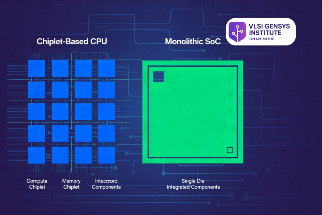
What Exactly is a Chiplet-based Design?
Think of it as moving from a monolithic skyscraper to a well-planned, modular campus.
A chiplet is a small, individual die that performs a specific function. A chiplet-based design, often called heterogeneous integration, involves assembling multiple of these chiplets onto a single, larger carrier—an interposer or a substrate—to create a single, functional system. This is the heart of advanced packaging technologies like 2.5D and 3D integration.
A typical chiplet system might look like this:
- One Chiplet: A high-performance CPU core built on a cutting-edge 3nm process.
- Another Chiplet: A GPU optimized for graphics, on a slightly older but more cost-effective 6nm node.
- Another Chiplet: An I/O and memory controller chiplet, perhaps on a 12nm node.
- All of these are connected via a high-speed, ultra-short interconnect (like Intel’s AIB or UCIe) on a silicon interposer, which acts like a super-highway for data between the chiplets.
The Compelling Advantages: Why the Industry is Buzzing
For VLSI students and professionals, this shift is a game-changer. Here’s why:
- “Mix-and-Match” Heterogeneity: This is the killer feature. You are no longer forced to build every component on the same, expensive technology node. You can use the best process for the specific function—a leading-edge node for logic, an older node for analog/RF, and a specialized node for memory. This optimizes performance, power, and cost simultaneously.
- Improved Yield and Lower Cost: Smaller dies have a significantly higher probability of being defect-free. By breaking a large monolithic die into smaller chiplets, you dramatically increase the yield. You can also manufacture high-volume, generic chiplets (e.g., I/O chiplets) and re-use them across multiple products, spreading out the NRE (Non-Recurring Engineering) costs.
- Faster Time-to-Market and IP Reuse: Instead of designing a massive new SoC from scratch for every product, companies can create a “chiplet library.” Need a new processor? Simply assemble it from pre-designed and pre-validated chiplets for CPU, GPU, and I/O. This slashes design cycles from years to months.
- Scalability and Modularity: Want to create a more powerful server CPU? Add more compute chiplets. Need a different GPU for a new market? Swap the graphics chiplet. This modularity offers unprecedented design flexibility.
The Inevitable Challenges: It’s Not All Smooth Sailing
Of course, this new paradigm introduces a fresh set of complex engineering puzzles:
- Packaging and Interconnects: The magic lies in the interconnect. The communication between chiplets must be incredibly fast, low-latency, and power-efficient. Standards like the Universal Chiplet Interconnect Express (UCIe) are emerging to create an ecosystem where chiplets from different vendors can “talk” to each other seamlessly. Packaging itself becomes a critical part of the design, moving from a final step to a core discipline.
- Thermal and Power Integrity: Having multiple power-dense chiplets in close proximity creates complex thermal hotspots. Managing power delivery and heat dissipation across the entire package is a significant challenge.
- Testing and Debugging: How do you test individual chiplets before assembly? How do you debug a system where the fault could be in a chiplet, the interposer, or the interface? Test strategies become far more complex.
- Ecosystem and Standards: For chiplets to truly flourish, a robust ecosystem with standardized interfaces (like UCIe) is essential. We are moving from a world of integrated design to a world of collaborative, multi-vendor assembly.
So, Is This the End for the Monolithic SoC?
The short answer is no, but its reign is changing.
The monolithic SoC is not going to vanish. For many applications—especially mobile and embedded systems where extreme power efficiency and compact form factors are paramount—a monolithic design will remain the optimal solution.
However, for the high-performance computing (HPC), data center, and advanced networking markets, where performance and scalability are pushing the limits of physics and economics, the chiplet-based approach is undoubtedly the future.
Conclusion: A New Playbook for VLSI Engineers
The shift to chiplets is more than just a technological change; it’s a philosophical one. It marks a transition from “How small can we make this transistor?” to “How intelligently can we assemble these functional blocks?”
For VLSI students and professionals, this opens up exciting new frontiers. Expertise is no longer confined to transistor-level design and physical design of a single die. The future demands knowledge in:
- Advanced packaging (2.5D/3D)
- High-speed serial links and interconnect protocols
- System-level architecture and co-design
- Thermal and power integrity analysis at the package level
The monolithic SoC was a brilliant solo. The chiplet-based system is a sophisticated orchestra. The question is no longer about which one will “win,” but about learning the new instruments and the conductor’s score to build the next generation of silicon marvels. The concert is just beginning.

One Response