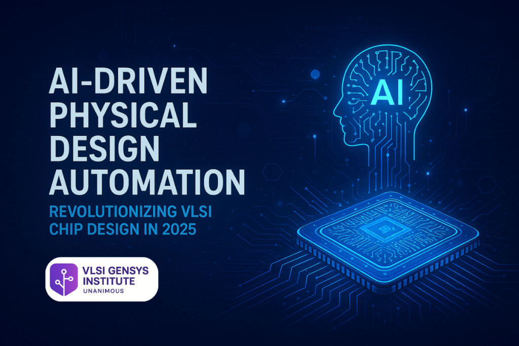
In the ever-evolving world of Very Large Scale Integration (VLSI), the demand for faster, smaller, and more efficient chips is pushing the boundaries of traditional design processes. Physical design automation, a crucial stage in chip manufacturing, has historically relied on rule-based algorithms and heuristics to arrange millions of transistors on silicon. However, the introduction of Artificial Intelligence (AI) is transforming this landscape, bringing a new era of efficiency and innovation to VLSI design.
This blog explores how AI-driven physical design automation is changing the game, its benefits, challenges, and what it means for engineers and the semiconductor industry in 2025 and beyond.
What is Physical Design Automation?
Physical design automation involves converting a chip’s logical design into a physical layout, ready for fabrication. It includes stages like placement, routing, clock tree synthesis, and timing optimization. The goal is to optimize power, performance, and area (PPA) while meeting design constraints.
Traditionally, physical design has been guided by Electronic Design Automation (EDA) tools employing handcrafted rules and heuristics. These methods work well but become increasingly strained when dealing with the complexity of modern chips designed at advanced nodes such as 3nm or below.
How AI is Integrating with Physical Design
Artificial Intelligence, particularly machine learning (ML) and deep learning (DL), offers powerful alternatives to traditional approaches. By learning from extensive design data, AI models can predict and optimize complex design parameters far more efficiently.
AI for Placement and Routing
Placement—deciding the exact locations of standard cells—and routing—connecting these cells with metal wires—are two of the most challenging phases. AI algorithms can analyze vast datasets of previous layouts to detect patterns and relationships that escape conventional heuristics.
For instance, reinforcement learning (RL), a subset of AI, allows algorithms to simulate millions of placement and routing attempts, learning strategies that result in optimal layouts. This reduces design iterations, shortens cycle times, and improves chip quality.
Predictive Analytics and Design Space Exploration
AI models enhance design space exploration by predicting design outcomes based on input parameters, enabling early identification of bottlenecks like timing violations or congestion. This predictive power helps engineers adjust constraints dynamically, leading to smarter decisions and more robust designs.
Self-Learning EDA Flows
One of the most exciting developments is self-learning EDA workflows. These systems use continuous feedback from design outcomes to refine their algorithms without human intervention, adapting to new technology nodes and design styles with minimal manual tuning.
Key Benefits of AI-Driven Physical Design Automation
Speed and Productivity Boost
AI cuts down design cycle times drastically by automating repetitive and complex tasks. The rapid convergence on optimal solutions means products reach the market faster, a critical advantage in the fiercely competitive semiconductor industry.
Improved Design Quality
By leveraging large datasets and learning from past designs, AI reduces human error and speculative trial-and-error, resulting in layouts with better power efficiency, performance, and smaller silicon area.
Scalability to Advanced Nodes
With chip geometries shrinking rapidly, traditional methods struggle to keep up with new constraints and complexities. AI’s adaptability makes it ideal for handling the unique challenges of 3nm and beyond nodes, including increased variability and manufacturing defects.
Challenges and Considerations
While AI offers tremendous promise, its adoption in physical design automation also faces challenges:
- Data Quality and Quantity: AI models require extensive, high-quality data for training. Access to diverse datasets that cover various design styles and process nodes is critical.
- Interpretability: Many AI solutions, especially deep learning models, behave like “black boxes,” making it challenging for engineers to understand decision-making processes and verify correctness fully.
- Integration with Existing Flows: Seamlessly incorporating AI into established EDA workflows requires compatibility and standardization efforts.
Real-World Applications and Case Studies
Several leading semiconductor companies and EDA tool vendors have begun integrating AI into their physical design tools. For example, AI-powered placement engines have demonstrated improvements in reducing total wire length and timing violations in complex SoCs.
At VLSI Gensys Institute, we constantly explore these cutting-edge developments to train engineers on the practical application of AI in VLSI design. To understand more about the latest trends in VLSI design and automation, you can check out our detailed articles on VLSI design methodologies.
The Future of Physical Design with AI
Looking ahead, AI will not merely assist but likely lead the physical design process. Advances in generative AI, foundation models trained on vast chip layout data, and self-optimizing systems are envisioned to make design nearly autonomous.
Moreover, ethical considerations and transparency in AI-driven design decisions will become increasingly important as AI’s role deepens.
Conclusion
AI-driven physical design automation is reshaping the semiconductor industry’s core, offering unprecedented efficiency, quality, and scalability. As chips become more complex and demands for speedier time-to-market grow, embracing AI in physical design workflows is not just beneficial—it’s essential.
At VLSI Gensys Institute, we are proud to empower engineers and researchers with the latest AI tools, techniques, and knowledge to stay at the forefront of this revolution.
Explore our training programs and blogs to stay updated on VLSI and AI innovations at www.vlsigensys.com/blog.
