If you’ve been following semiconductor trends, you’ve likely heard the term “3D-IC” buzzing around. It sounds like something from science fiction—chips stacked vertically, creating towering structures of silicon. But what does it really mean for VLSI students and professionals? Is this just another packaging fad, or is it the fundamental architectural shift experts claim it to be?
Let’s demystify 3D-IC together. This guide will walk you through the basics, the why, the how, and what it means for your career.
Beyond Moore’s Law: The Driving Force Behind 3D-IC
For decades, the industry happily rode the wave of Moore’s Law, shrinking transistors and packing more functionality onto a single, “monolithic” chip. But as we hit the 5nm node and beyond, the challenges have become monumental.
- Physical Limitations: Quantum effects and atomic-scale manufacturing introduce variability and leakage.
- Economic Limitations: The cost of building a new fabrication plant for cutting-edge nodes is astronomical.
- The “Memory Wall”: The speed of processors has vastly outpaced the speed of memory access. Data transfer between the CPU and off-chip memory is a major performance bottleneck.
3D-IC, or 3D Integrated Circuit, is a direct response to these challenges. Instead of just making transistors smaller, we start stacking them vertically. Think of it as building a skyscraper instead of a sprawling single-story warehouse. This vertical integration is the next frontier in performance, power, and area (PPA) optimization.
What Exactly is a 3D-IC? It’s More Than Just Stacking
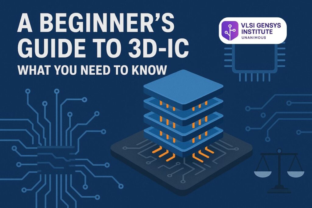
At its core, a 3D-IC is a chip architecture where multiple silicon dies (or “chiplets”) are integrated vertically into a single package. They are connected using through-silicon vias (TSVs) and micro-bumps, creating a dense, high-bandwidth interconnect.
It’s crucial to distinguish between different types of vertical integration:
- 2.5D Integration: This is often the gateway to 3D. Chiplets are placed side-by-side on a passive silicon interposer. This interposer has tiny wiring that allows the chiplets to communicate with very high bandwidth and low power. It’s like placing separate houses on a shared, high-speed street network.
- 3D Integration: This is the true “skyscraper” approach. Dies are stacked directly on top of one another. They are connected using Through-Silicon Vias (TSVs)—vertical electrical connections that pass completely through a silicon wafer or die. This allows for the shortest possible data paths between, for example, a processor and its memory.
The Nuts and Bolts: Key Technologies Enabling 3D-IC
To understand 3D-IC, you need to be familiar with the key technologies that make it possible.
1. Through-Silicon Vias (TSVs)
TSVs are the vertical elevators of the 3D-IC. They are microscopic, copper-filled holes that are etched through the silicon die and filled with a conductive material. They provide a direct electrical connection from the top of a die to the bottom, allowing for signals and power to travel between stacked layers. Compared to long, horizontal on-chip wires, TSVs offer orders of magnitude lower latency and power consumption.
2. Silicon Interposers (for 2.5D)
The interposer is the “middle-man” in a 2.5D configuration. It is a slice of silicon, but it doesn’t contain any active transistors. Instead, it’s packed with a dense mesh of interconnects. Chiplets are mounted on top of it, and the interposer routes traffic between them with much higher efficiency than a traditional organic substrate.
3. Micro-bumps and Hybrid Bonding
These are the ultra-fine “glue” that connects one die to another or to the interposer. Micro-bumps are much smaller than traditional solder bumps, allowing for a much higher connection density. The cutting-edge technology is hybrid bonding, which creates a direct, copper-to-copper bond between dies, enabling even finer pitches and better performance.
Why Bother? The Tangible Benefits of Going 3D
For a system architect, 3D-IC isn’t just a cool trick; it’s a toolbox for solving fundamental problems.
- Heterogeneous Integration: This is the superstar benefit. You can mix and match different process technologies optimally. Imagine stacking a high-performance 5nm CPU die directly on top of a mature, cost-effective 28nm analog/RF die and a specialized 7nm GPU die. You get the best of all worlds without compromise.
- Massive Bandwidth & Reduced Latency: By stacking a processor core directly on top of a memory die (like High-Bandwidth Memory – HBM), you replace slow off-chip communication with thousands of ultra-fast vertical TSV connections. This shatters the “memory wall” and is a game-changer for AI/ML and data-centric applications.
- Form Factor & Power Reduction: Shorter interconnects mean less capacitance and resistance, which directly translates to lower power consumption for the same performance. The compact footprint is also critical for mobile and IoT devices.
The Inevitable Challenges: A Reality Check for Designers
Transitioning to 3D-IC is not a simple plug-and-play. It introduces a new layer of complexity that VLSI engineers must grapple with.
- Thermal Management: Heat naturally rises. In a 3D stack, the top die effectively “cooks” the die beneath it. Managing these thermal hotspots is one of the most significant challenges. Sophisticated thermal modeling and new cooling solutions are non-negotiable.
- Design Complexity and EDA Tools: Traditional EDA tools were built for 2D design. 3D-IC requires new tools for multi-die co-design, partitioning, and TSV placement. Analyzing timing, power, and signal integrity across multiple dies is exponentially more complex.
- Test and Yield: How do you test a die that will be buried in the middle of a stack? If one die in a 10-die stack is faulty, the entire stack may be useless. New strategies for Known Good Die (KGD) testing and built-in self-test (BIST) are critical.
- Cost: The advanced packaging processes (TSV etching, thinning, stacking) are expensive. While it can be cheaper than a monolithic die at advanced nodes, the overall cost is still a significant factor.
What This Means for VLSI Professionals
The rise of 3D-IC is reshaping job roles and required skill sets. It’s no longer enough to be an expert in only front-end or back-end design. The future belongs to those who understand:
- System-Level Architecture: Thinking in terms of system partitioning and heterogeneous integration.
- Multi-Physics Analysis: Co-designing for thermals, power, and signal integrity from day one.
- Advanced Packaging: Familiarity with TSVs, interposers, and different bonding techniques.
Conclusion: The Third Dimension is Here to Stay
3D-IC is not a distant future technology; it’s already here, powering the world’s most advanced FPGAs, GPUs, and AI accelerators. While the monolithic SoC will remain relevant for many applications, the high-performance computing frontier is unequivocally moving into the third dimension.
For students and professionals, embracing 3D-IC means investing in the skills that will define the next era of semiconductor innovation. It’s a challenging but incredibly exciting field that promises to keep the spirit of Moore’s Law alive, not by making things smaller, but by making them smarter, taller, and more integrated than ever before. The sky is no longer the limit—it’s the foundation.
